- Home
- Innovations
- Technology Transfer & Networking
- Technologies
- LASER-INDUCED SELECTIVE PLATING OF DIELECTRICS FOR ELECTRONIC CIRCUIT FABRICATION
LASER-INDUCED SELECTIVE PLATING OF DIELECTRICS FOR ELECTRONIC CIRCUIT FABRICATION
DESCRIPTION, INNOVATION AND ADVANTAGES
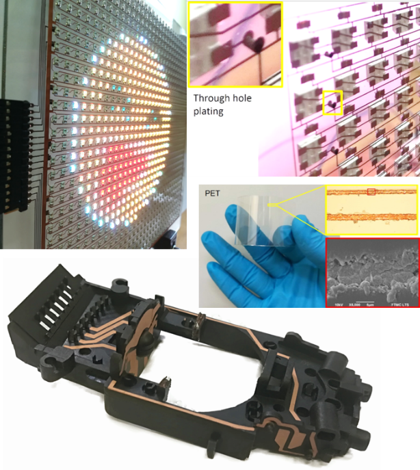
Electric circuit traces formation on 3D shaped dielectrics is one of the biggest challenges in 3D Mechatronic Integrated Devices (3D-MID). The advanced technology of Selective Surface Activation Induced by a Laser (SSAIL) can solve emerged production issues for electric traces. The process can be applied almost on any commercial dielectric material by adapting laser and chemical parameters. Narrow copper lines below one micrometre in a width) are feasible to produce. The technology is capable to fabricate a metallic mesh with metal wires less than 5 µm in diameter to be invisible but still electro-conductive. Therefore, such metallic mesh can substitute Indium Tin Oxide (ITO) in the transparent conductive film market.
CURRENT STAGE OF DEVELOPMENT
Ready for the integration in production lines.
STATUS OF INTELLECTUAL PROPERTY RIGHTS
Patented (WO 2018051210; JP 6749482; LT 6518; US 10982328; EP 3512980; CN 109844178; KR 102319221
TYPE AND ROLE OF PARTNER SOUGHT
- Industrial Electronics manufacturers.
- Partners for global marketing.
CONTACT
Dr. Karolis Ratautas
Phone +370 618 42061; e-mail: karolis.ratautas@ftmc.lt