- Home
- News & Events
- News

Breakthrough Electromagnetic Wave Absorber Developed by International Team Featured on the Back Cover of Advanced Optical Materials
Researchers from the FTMC have received another international recognition: the prestigious Advanced Optical Materials has published their article illustrated on the back cover.
A team from the FTMC Department of Optoelectronics – Dr Irmantas Kašalynas, Dr Saulius Tumėnas, Dr Justinas Jorudas, Dr Andrzej Urbanowicz, Dr Vytautas Janonis, Dr Daniil Pashnev and Dr Surya Revanth Ayyagari – together with colleagues from the University of Eastern Finland and the University of Tokyo, have developed a universal electromagnetic wave absorber, which could find applications in fields such as space research and defence.
What makes this technology special – and what do insect eyes have to do with it?
A World First
As the name suggests, an electromagnetic wave absorber is a device that “captures” certain invisible waves, preventing them from spreading into the surrounding environment.
Perhaps the simplest analogy would be a sound recording studio, where musicians perform their latest hit: the studio walls are lined with special materials that absorb sound waves, eliminating any echoes and ensuring a clean recording.
FTMC has a similar facility: the Microwave Anechoic Chamber in the Department of Physical Technologies is lined with fibrous “spikes” that absorb microwaves. This enables experiments with various antennas, smart devices, drones and other technologies that rely on such waves.

(Dr Irmantas Kašalynas. Photo: Hernandez & Sorokina / FTMC)
However, there has always been a challenge – specific absorbers typically work only within a narrow electromagnetic range, and a truly universal device had not been created. Until now.
“Our work stands out because we have developed an absorber that operates across a spectrum stretching from terahertz waves to the deep ultraviolet region. That is an exceptionally wide range – a global first,” says one of the paper’s authors, Dr Irmantas Kašalynas, Head of the Terahertz Photonics Laboratory at FTMC Department of Optoelectronics.
He adds that research is ongoing, with the device’s technical details still being refined. The absorber itself is a small black object that becomes far more intriguing under a microscope: its surface resembles a neatly trimmed forest of thuja trees, and when magnified further, one can see sharp-tipped pyramids. These “spikes” are what enable the absorption of electromagnetic waves.
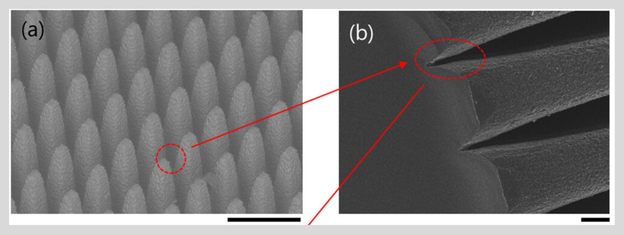
(Scanning Electron Microscope (SEM) images of the moth-eye/PyC structure at different magnifications. For comparison: (a) shows an area about a thousand times smaller than the width of a human hair, and (b) about five thousand times smaller. Photos: FTMC)
“Simply put, it’s a silicon wafer whose surface has been engineered into what’s called a moth-eye structure – it really does resemble an insect’s eye. This structure reduces the refractive index, easing the transition of electromagnetic waves from air into the material. The result is less reflection and greater transparency, as more light can enter.
The moth-eye structure is also used in optical plates, lenses, and anti-reflective coatings on glass – similar to the films used on phone screens,” explains Dr Kašalynas.
The Advantage of Being Black
The key innovation achieved by the Lithuanian and international team lies in adding a layer of pyrolytic carbon to the moth-eye surface. This combination turned the structure completely black – making it suitable for an exceptionally wide range of electromagnetic waves.
“This blackness means our material absorbs visible, infrared and terahertz radiation alike. There are very few substances in nature that behave this way – so this is a truly unique result. You could say that nothing passes through it and nothing reflects from it. It’s absolute black night,” says the researcher.
On the back cover of Advanced Optical Materials, the illustration depicts waves of different ranges (from the top) – deep ultraviolet, visible light, infrared and terahertz – being absorbed into the black, spiked material. The image, created by a Swiss design company, perfectly captures the absorber’s operating principle.
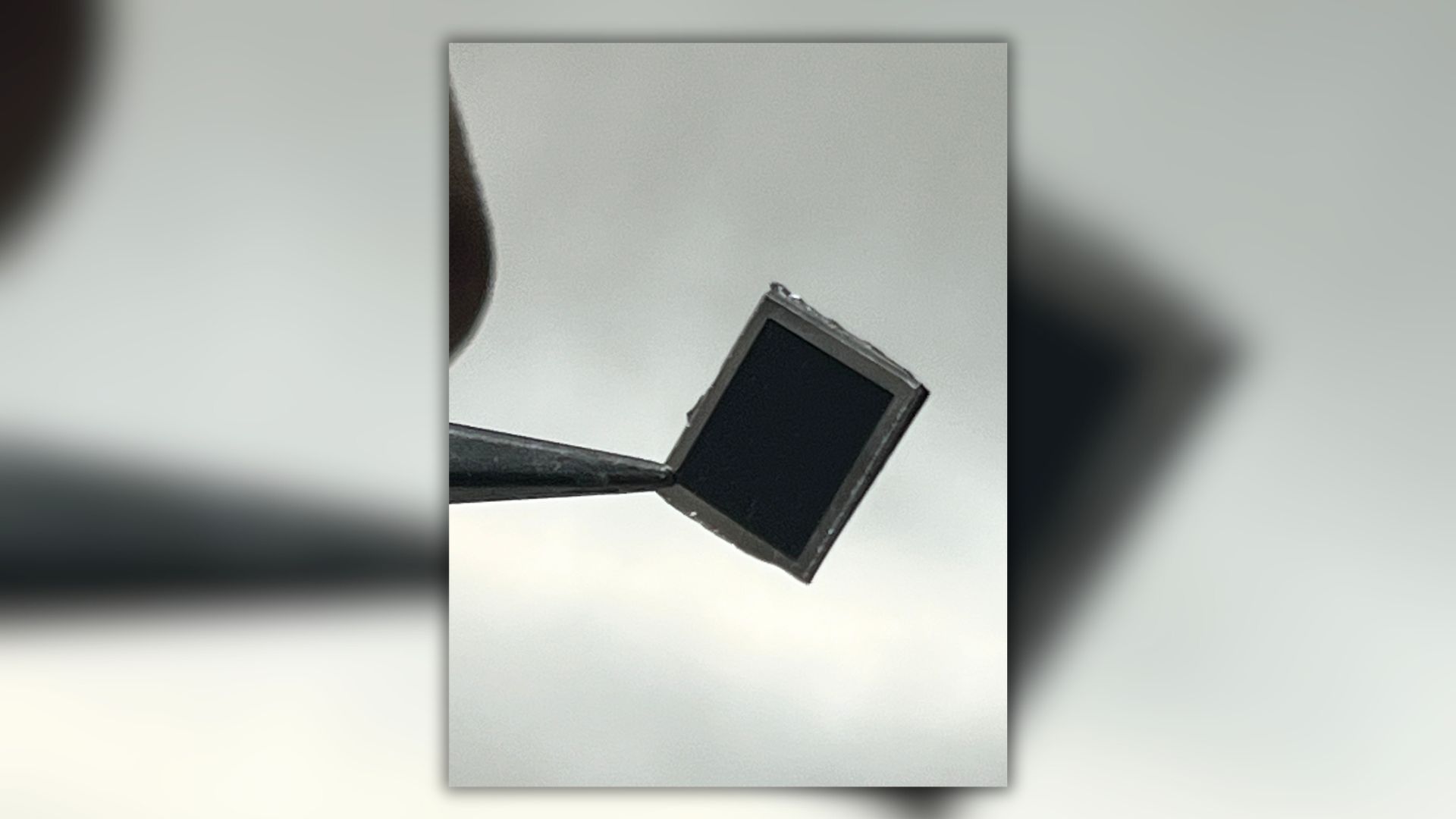
(Carbon-coated moth-eye sample. Photo: University of Tokyo)
According to the FTMC scientist, each institution contributed its expertise: the Japanese partners developed the moth-eye silicon surface, the Finnish researchers coated it with a carbon thin layer responsible for the material’s blackness, and our team emploing various advanced techniques performed precise measurements and data interpretation.
“Such absorbers are of interest for calibrating instruments and studying material surfaces. Our partners at the University of Tokyo see potential use in space research – in astronomical instruments and radio telescopes. These devices require surfaces that can absorb waves within specific spectral bands.
Moreover, the European Union is increasingly linking space and defence research, so this material is of interest to both areas. Perhaps one day we’ll even have a fully ‘black’ test chamber – it’s still very costly at the moment, but it would be fascinating,” concludes one of the study’s authors Kašalynas.
This research at FTMC was supported by the EU H2020 programme ITN-MCS project "Terahertz Photonics for Communications, Space, Security, Radio-Astronomy, and Material Science" (TERAOPTICS) under the agreement No. 956857.
Written by Simonas Bendžius