- Home
- News & Events
- News
ELI Conference Highlights Lithuania’s Strategic Role in Photonics and Semiconductor Innovation
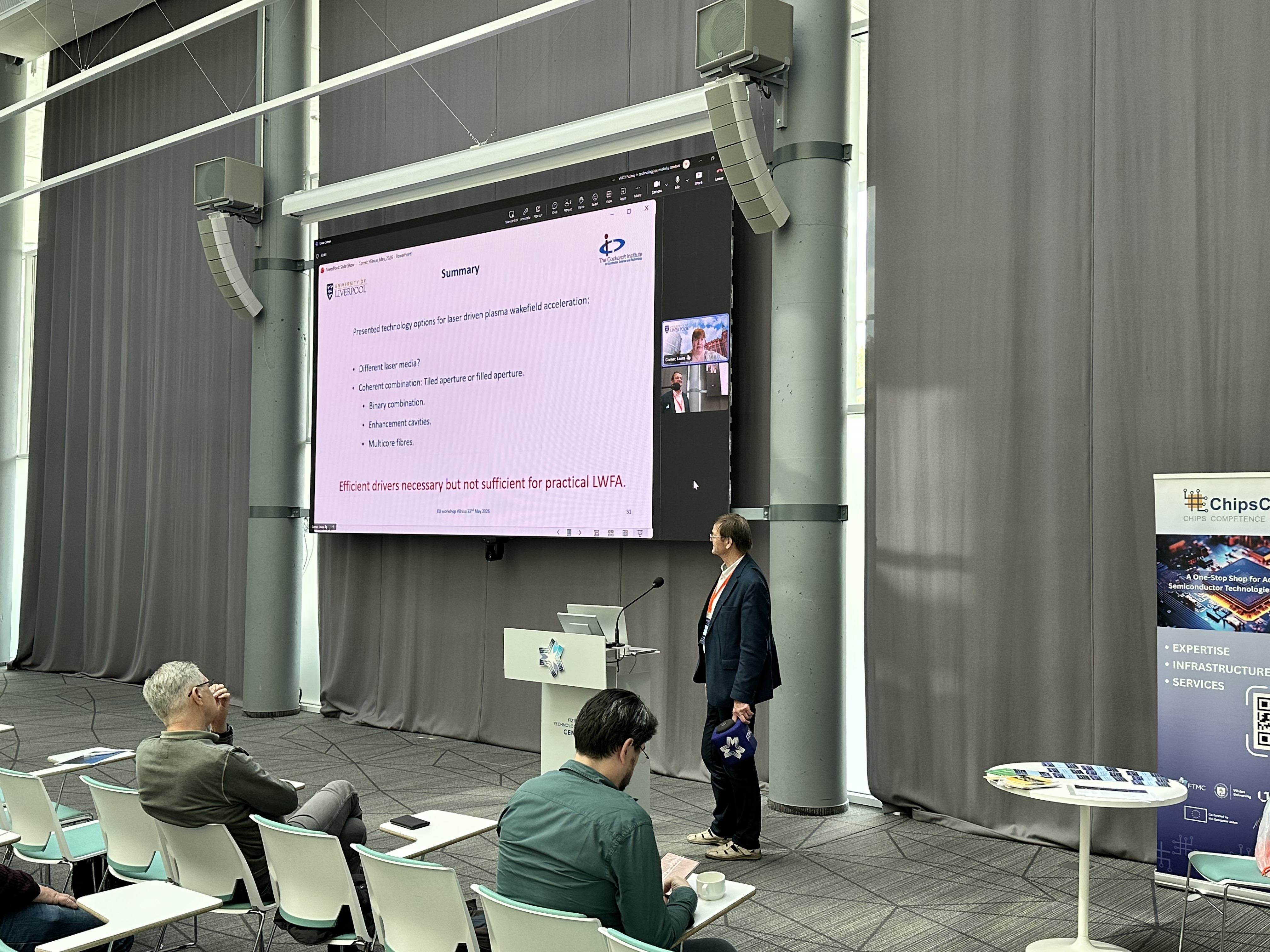
On May 21–22, an international workshop titled “Laser-Driven Particle Accelerators, Their Applications and Experimental Opportunities within the ELI Infrastructure” took place at the Center for Physical Sciences and Technology (FTMC) in Vilnius, Lithuania. The two-day event brought together researchers from across Europe to discuss the latest advances in laser-driven particle beams and their applications in fundamental science, industry, and medicine.
The workshop also became an important platform for discussing how Lithuania’s strong laser photonics ecosystem can contribute to the rapidly growing semiconductor sector in Europe.
ELI Infrastructure Opens New Opportunities for Lithuanian Researchers
The event began with presentations from representatives of the three major facilities of the European Extreme Light Infrastructure (ELI ERIC): ELI Beamlines (Czech Republic), ELI-NP (Romania), and ELI ALPS (Hungary).
Speakers introduced open-access opportunities available to international research teams, including advanced secondary source platforms such as laser-driven X-rays, neutron beams, accelerated electrons, and proton sources. These capabilities create new experimental opportunities for research groups at FTMC and Vilnius University working in laser acceleration and high-field physics.
Expanding Applications: Radiotherapy, Neutrons, and Biomedical Research
The first day also focused on biomedical and medical applications of laser-accelerated particles. Presentations covered FLASH radiotherapy experiments conducted by French and Lithuanian researchers, activities of the “LT Radiomed” consortium, and neutron irradiation studies performed at ELI ALPS.
These discussions demonstrated how ELI infrastructure is becoming increasingly important not only for physics research but also for interdisciplinary biomedical innovation.
Automation, Advanced Optics, and Synchrotron Integration
On May 22, the program highlighted automated physics experiments and advanced laser optics. Researchers from Munich University presented machine learning approaches for optimizing laser-plasma experiments, while DESY scientists introduced plasma injector developments for the PETRA IV synchrotron.
FTMC researchers showcased betatron X-ray generation using a two-stage plasma target, and participants visited FTMC Laser Technologies laboratories to explore the latest photonics innovations developed in Lithuania.
Photonics and Semiconductors: A Strategic Technological Synergy
A particularly relevant presentation for the semiconductor sector was delivered by researchers from Vilnius University’s Department of Semiconductor Physics. Their talk, “Semiconductor Detectors for High-Energy Particles and Beams,” introduced advanced silicon-based detector systems designed for precise measurements of laser-accelerated particle beams.
The topic directly aligns with semiconductor-related activities implemented under the LASER PRO project at FTMC. The project aims to integrate ultrashort pulse laser technologies into microelectronics, nanoelectronics, and semiconductor manufacturing processes.
Importantly, semiconductor detectors are not only tools for experiments — they are themselves manufactured using femtosecond laser processing technologies. This creates a two-way technological relationship: lasers help fabricate semiconductor detector structures, while detectors measure laser-generated particle beams.
Today, photonics is inseparable from semiconductor manufacturing. From extreme ultraviolet (EUV) lithography used in advanced chip fabrication to laser-based wafer cutting and defect inspection systems, modern chips could not exist without photonics technologies. Increasingly, semiconductor devices also integrate photonic components for high-speed data transmission and optical interconnects.
ChipsC²-LT: Strengthening Lithuania’s Semiconductor Ecosystem
By expanding its semiconductor capabilities, FTMC is leveraging Lithuania’s internationally recognized strengths in lasers, THz technologies, and photonics while developing new competencies aligned with European Union priorities.
To support this vision, the Lithuanian Chips Competence Centre, ChipsC²-LT, was established. Coordinated by FTMC together with national partners, the initiative contributes to the implementation of the European Chips Act in Lithuania.
ChipsC²-LT focuses on four strategic areas:
- Chip design
- Power electronics
- Heterogeneous integration
- Photonic integrated circuits (PICs)
The ELI workshop demonstrated how these fields increasingly converge in practice. Semiconductor detector technologies, advanced photonics, laser systems, and accelerator science together form a multidisciplinary ecosystem capable of creating significant competitive advantages for Lithuania within the European semiconductor landscape.
Photonics has long been one of Lithuania’s strongest high-technology sectors. As the global semiconductor industry increasingly depends on photonics solutions, Lithuania’s expertise gains growing strategic importance for Europe’s future semiconductor ecosystem.
Projects such as LASER PRO and ChipsC²-LT provide a strong foundation for transforming this scientific excellence into technological innovation, industrial growth, and long-term economic impact.
More information:
www.laserpro-eh.eu
www.chipsc2.lt