- Home
- News & Events
- News
Towards a Dream: FTMC Physicist Dr Rokas Kondrotas Begins a Research Fellowship at One of the World’s Leading Universities, MIT
The Massachusetts Institute of Technology (MIT) is one of the most renowned universities in the world and an influential centre for innovation and technological development.
In various prestigious global university rankings, MIT consistently places first or second, and over its more than 160 years of existence, the institution has produced more than a hundred Nobel Prize laureates. Gaining admission to study, undertake a placement, or work there is extremely difficult, so when a Lithuanian succeeds, such news can be considered an achievement not only for the individual but for Lithuania as a whole.
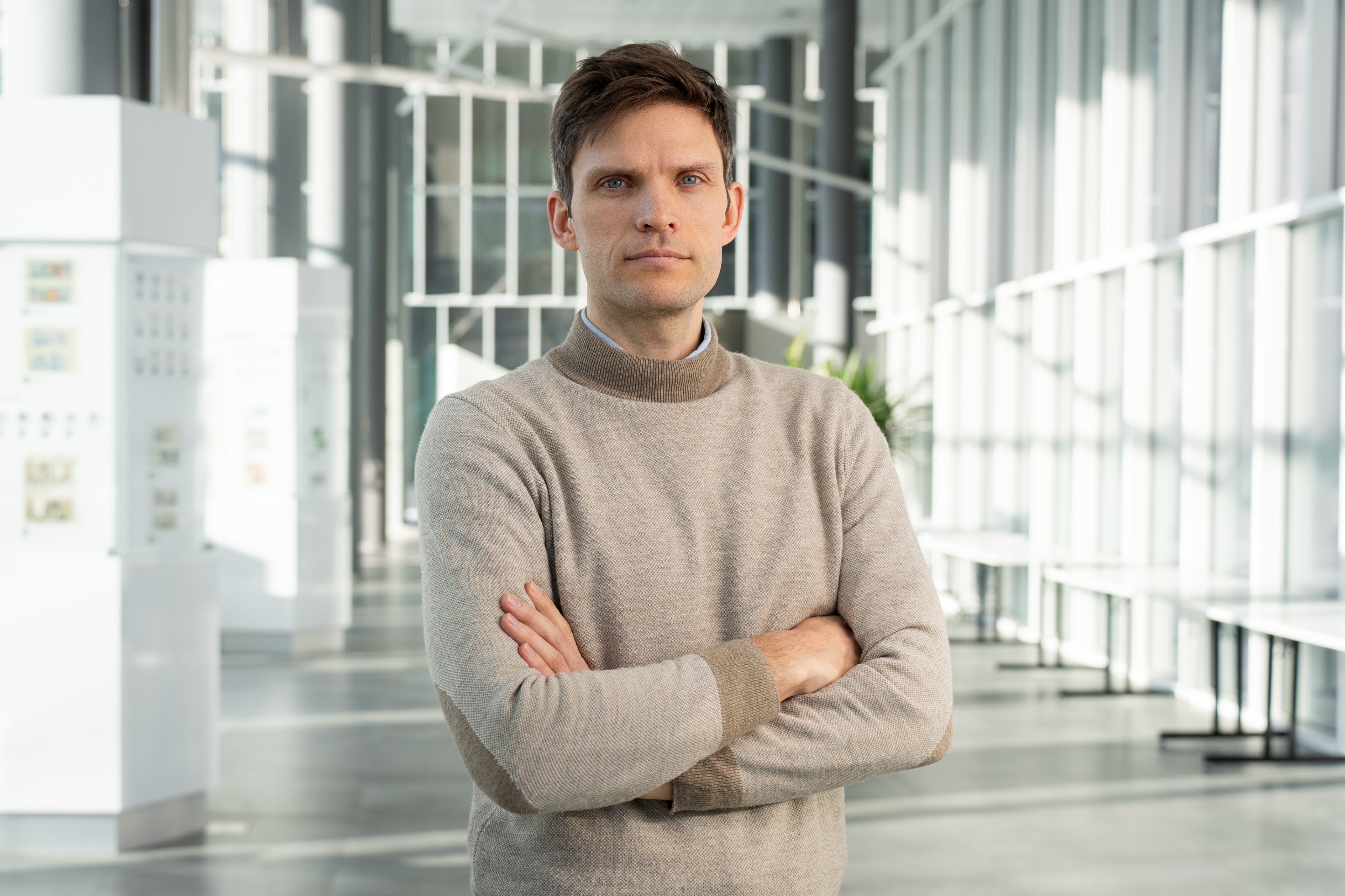
From June, Dr Rokas Kondrotas, a physicist at the FTMC Department of Characterisation of Materials Structure, began a research fellowship at MIT. At this prestigious university, he will work in the Department of Materials Science and Engineering, where he will grow and study compounds of the chemical elements selenium and tellurium. He will seek to apply these materials in the development of advanced sensors for autonomous vehicles as well as in next-generation solar cells.
This opportunity has been provided to the Lithuanian researcher by the Baltic-American Freedom Foundation (BAFF), which encourages scientific collaboration between the United States and the Baltic states. BAFF invites talented individuals to study and undertake fellowships in the US and covers their financial costs.
Many scientists would consider the opportunity to work at MIT the fulfilment of a dream, yet Dr Kondrotas is already planning ahead and aiming for another achievement: the physicist hopes that this invaluable experience will strengthen his chances when applying for the prestigious European ERC Grant, which provides researchers with a solid foundation for realising their scientific goals.
We spoke to the FTMC scientist in more detail about this.
.jpg)
(MIT. Photo: Canva.com)
How did the opportunity to undertake a fellowship at MIT arise?
A year ago, I first heard about BAFF. I investigated the opportunities they offer and chose the Research Scholar Program.
I am very pleased about this – there are now many different programmes for PhD students or postdoctoral fellowships, but there are almost none for more senior researchers. And BAFF explicitly states that it is aimed at more experienced, somewhat advanced researchers. It opened a very good opportunity to gain new knowledge and competencies.
Before submitting my application, last summer I intensively searched for an institution in America that would be willing to host me. MIT was among those I approached. I wrote to Professor Rafael Jaramillo, whose presentation on a topic like mine I had heard at a conference. After reading about my idea – growing and studying selenium–tellurium compounds – he was initially quite sceptical, but later, during a remote conversation where I explained more details about the project, his interest increased.
I then submitted my application to the Research Scholar Program in the US, and after passing the first selection round, I had an interview with BAFF representatives from Lithuania, Latvia and Estonia. They were surprised that I had managed to arrange an invitation from MIT, as it is rare for the university to accept people “from the outside” so easily. I replied that the stars had aligned – my future supervisor was interested in the idea, and he also had unused equipment that was ideally suited for growing and studying the materials I was interested in.
What will your working day look like in the MIT Department of Materials Science and Engineering?
I will be going to the laboratory, where, using a specialised molecular beam epitaxy system, I will grow selenium–tellurium layers and observe how their properties change under different growth conditions. I will study their structural and physical properties, and each time I will try to produce coatings of ever higher quality so that they are as suitable as possible for use in various sensors.
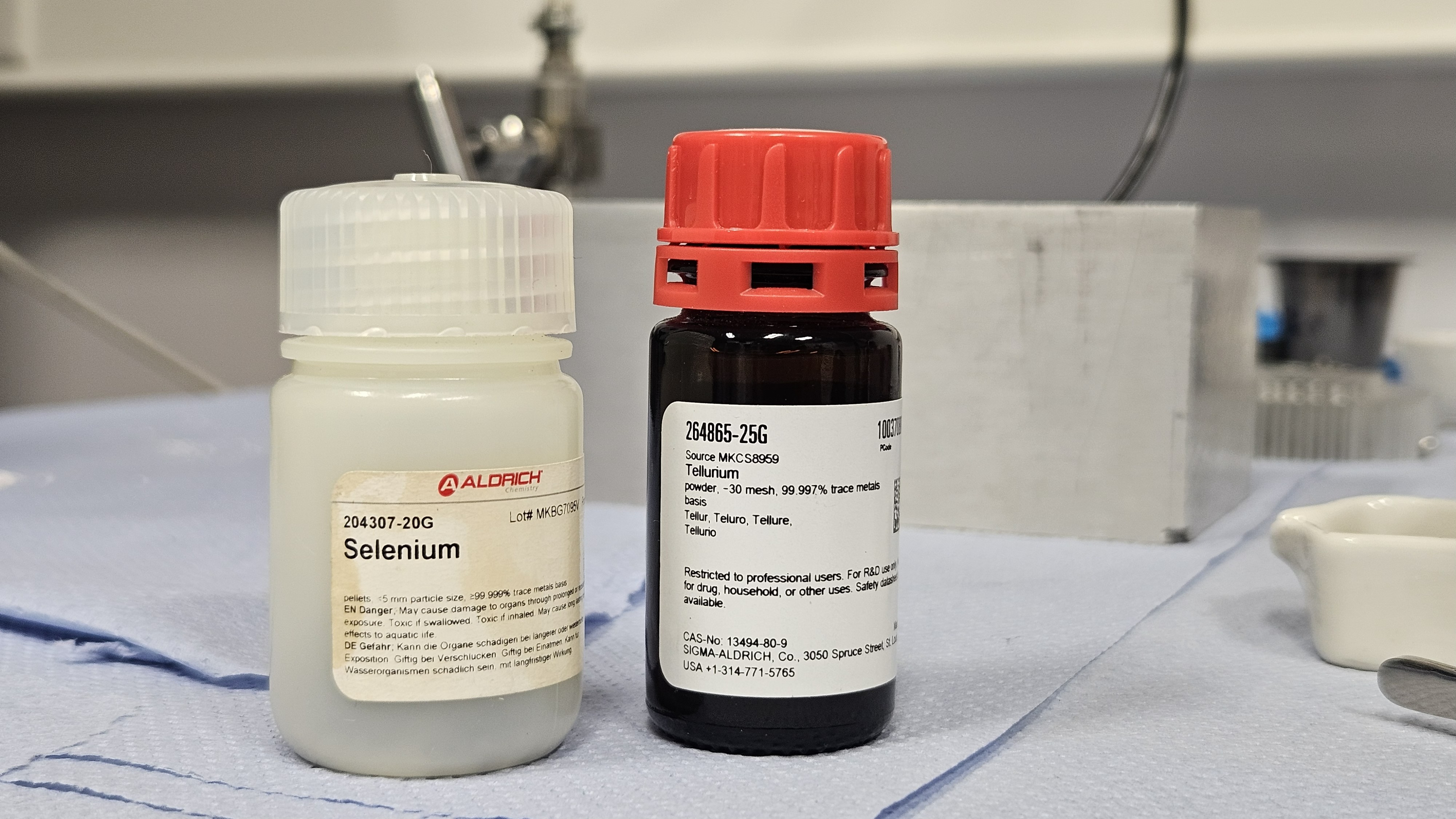
(Selenium pellets and tellurium powder. These two materials are expected to help drive a breakthrough in the fields of sensors and solar cells. Photo: FTMC)
Before discussing possible applications, could you briefly explain what selenium and tellurium are?
They are two chemical elements from the so-called chalcogen group, characterised by semiconductor properties. At MIT, I will grow and study them in the form of thin crystalline films. Selenium is, in fact, an essential micronutrient for human health, and incidentally, the very first solar cells were made on its basis more than 140 years ago. Tellurium, meanwhile, is like its “big brother”, more often studied in electronics, especially in the development of new types of transistors.
Pure selenium has insulating properties, whereas pure tellurium, on the contrary, is a semiconductor. By mixing these two elements, it is therefore possible to obtain selenium–tellurium compounds with a range of different properties. By better understanding their characteristics and growth mechanisms, this material could be applied in the development of advanced technologies.
What might those applications be?
The main focus will be on forming selenium–tellurium alloys operating in the spectral range from 1400 to 2500 nanometres, which belongs to the short-wave infrared (SWIR) region. This is light that is invisible to the human eye but is very useful for recognising objects in harsh weather conditions or at night. Because of these and other practical applications, I plan to study selenium–tellurium coatings and develop sensors that perform well specifically in the SWIR range.
The field of application for such sensors is quite broad, as this range is relevant both to science and industry. One of the most important areas could be assisting autonomous vehicles: when driving at night or in heavy fog, a car, so to speak, sees only as much as the person inside it. An integrated additional sensor would allow the vehicle to “see” its surroundings even in difficult weather conditions and help its system assess obstacles and hazards on the road.
It is true that various SWIR sensors have already been developed worldwide, and some are very good. In our case, we aim to grow polycrystalline coatings that would not require expensive substrates, and the technological process itself would be simpler. At the same time, by exploiting the unique properties of selenium–tellurium, we want to achieve sufficient sensor quality and high sensitivity. Such a sensor could be produced much more cheaply.
Another important application of SWIR is in night vision devices, which is significant for defence, for example in the development of autonomous drones.
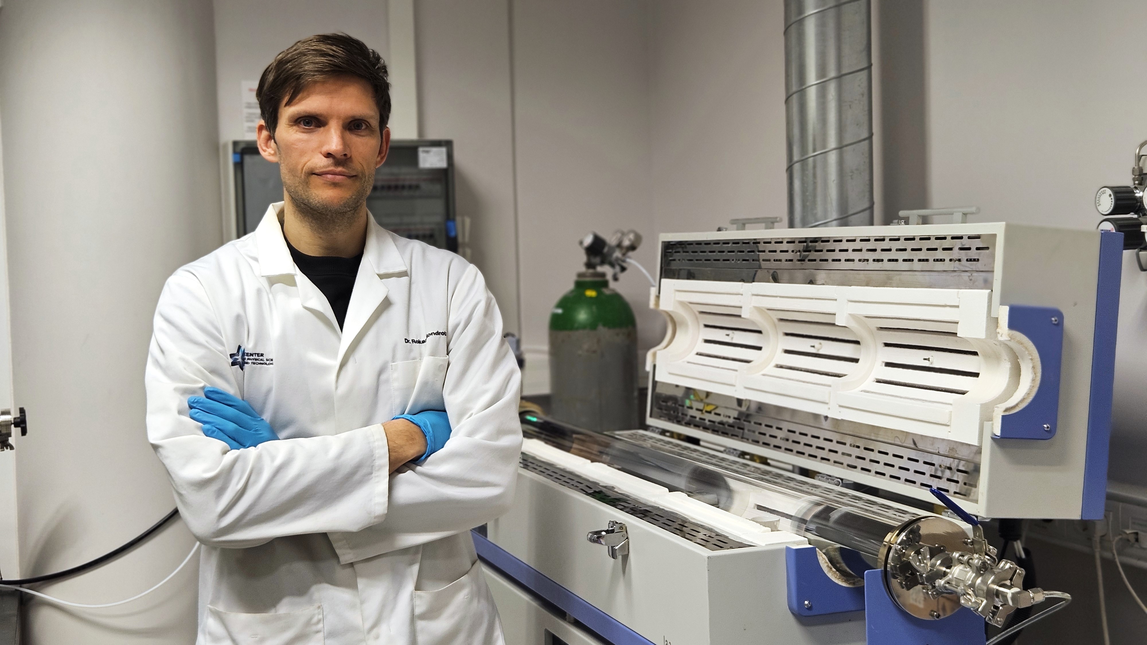
(Dr Rokas Kondrotas. Photo: FTMC)
One of the areas you are developing at FTMC is next-generation solar cells. Could selenium–tellurium compounds also be useful here?
I have been thinking about this for the past three to four years. At present, there is significant progress in so-called tandem solar cells, where two materials, silicon and perovskite, are combined. The top perovskite layer in silicon solar cells can theoretically increase their efficiency to as much as 43%, which is why this field is attracting a great deal of investment.
However, around 20% of solar energy is not absorbed by silicon or silicon–perovskite tandem cells. If we placed a material with suitable properties beneath the silicon element, it would be possible to further increase efficiency by about 5%.
In that case, we would obtain a three-layer structure: perovskite on top, silicon in the middle, and a third material at the bottom. Such a “sandwich” could theoretically achieve a record efficiency of almost 48%, and in practice one might expect close to 40%. However, it is very important to maintain a low cost – otherwise, such technology would be unaffordable for the average user.
Therefore, materials that exhibit good properties but are inexpensive to produce are particularly valued. Selenium–tellurium compounds, in my opinion, meet these criteria and are promising for the development of entirely new generations of solar cells or SWIR sensors. Interestingly, in scientific literature, the application of these materials in optoelectronics is still discussed relatively little.
Returning to MIT – what does the opportunity to test yourself at such a world-class university mean to you as a scientist?
First, I am incredibly pleased. I always seek to acquire new competencies and knowledge. A journey to such an almost utopian institution is a tremendous opportunity for me to learn, improve and broaden my horizons. I value that greatly and want to make the most of it.
For a long time, MIT seemed like a kind of “holy grail” or Mecca that one simply must visit. Perhaps I have romanticised it somewhat, but the name MIT certainly carries special weight. I recently shared this on my LinkedIn account – not to boast, but to show that such opportunities exist and to thank the organisation that made it possible.
I received many warm congratulations from old friends and colleagues – everyone understands very well the significance and prestige of the MIT name. Even if I do not move mountains there, being in such an institution is a very rewarding experience.
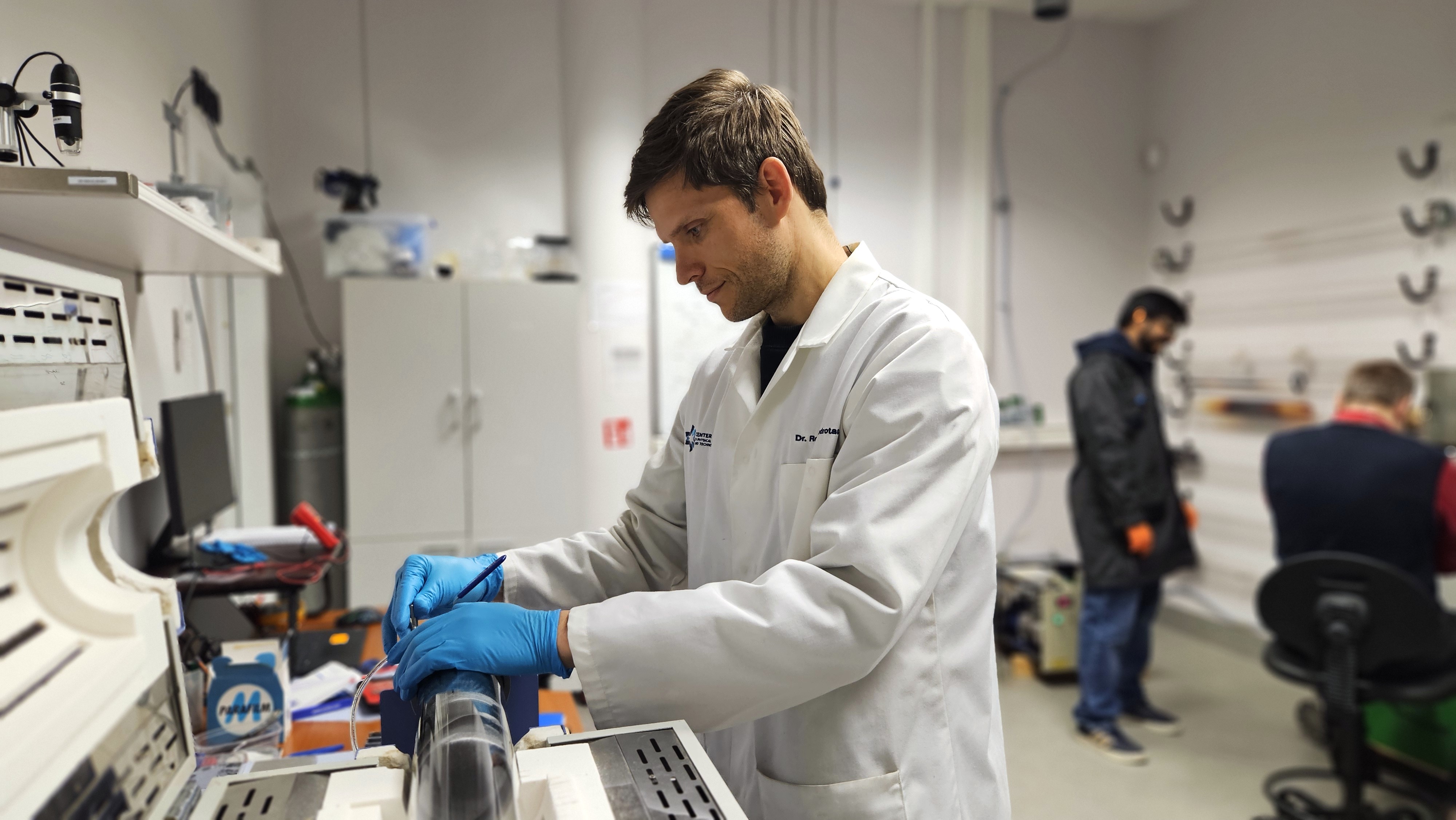
(Dr Rokas Kondrotas. Photo: FTMC)
Do you already have plans or ideas for what you will do when you return from the US next year with this new experience?
Yes, I have been working on a plan for some time. My goal is to strengthen my competencies, gain experience with selenium–tellurium materials, and after the fellowship, apply for a European Research Council (ERC) Grant. This is probably the most prestigious funding source for an individual scientist in Europe, allowing one to establish a research group and begin a new research direction.
Winning this grant is extremely difficult, with enormous competition. I have applied once before and was unsuccessful, but I believe that the additional experience gained at MIT could make a significant difference. In my previous application, I lacked evidence of sufficient practical experience. Next year, I will have more of it, as well as real scientific results in this field.
An ERC Grant essentially transforms a scientist’s career. It provides enormous financial freedom – around €2 million for research and about another €1 million for equipment. It is not only my dream but also that of many scientists. Such funding would allow me to acquire the latest equipment, attract talent, and develop a research direction that interests me in the fields of next-generation sensors and solar cells.
I very much hope that this dream will come true, and I am eagerly looking forward to starting my work at MIT.
Written by Simonas Bendžius