Innovations
- Home
- Innovations
- Technology Transfer & Networking
- Technologies
Technologies
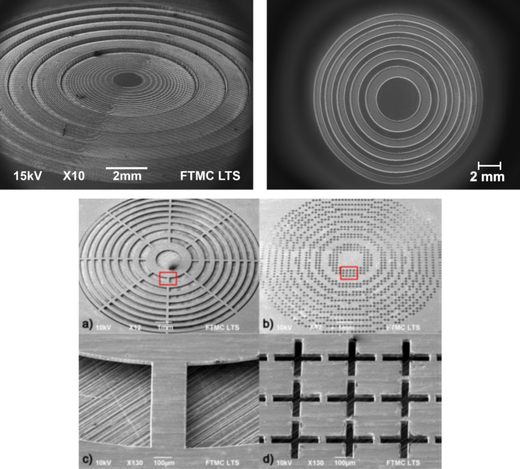
DEEP 3D LASER ENGRAVING TECHNOLOGY
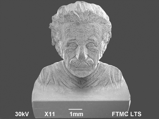

DESCRIPTION, INNOVATION AND ADVANTAGES
The technology can be applied for various materials processing. During the preparation stage, the 3D object drawing is divided into individual layers. Afterwards, layer by layer material ablation is introduced. The use of picosecond laser pulses for processing ensures high processing quality and speed. Compared to nanosecond lasers, the short pulse – matter interaction time significantly reduces the thermal effects. The laser-induced heat diffusion is limited at such pulse durations. Therefore, melt formation and oxidation of the surface are significantly reduced. Also, burr formation is much lower compared to nanosecond laser processing. In the case of copper, an 8 mm3/min ablation rate is achieved.
Materials: metals, semiconductors, ceramics, glass, polymers.
Ablation precision: 50 μm.
Ablation rate: 8 mm3/min (copper).
CURRENT STAGE OF DEVELOPMENT
Technology validated in small-series production.
INTELLECTUAL PROPERTIES RIGHTS STATUS
Know-how and design rules.
TYPE AND ROLE OF PARTNER SOUGHT
Companies producing mini-moulds, imprints with µm-scale structures.
CONTACT
Dr. Paulius Gečys
Phone +370 600 04346, e-mail: p.gecys@ftmc.lt
TRUE ZERO-ORDER WAVEPLATES BASED ON ALL-SILICA THIN FILMS
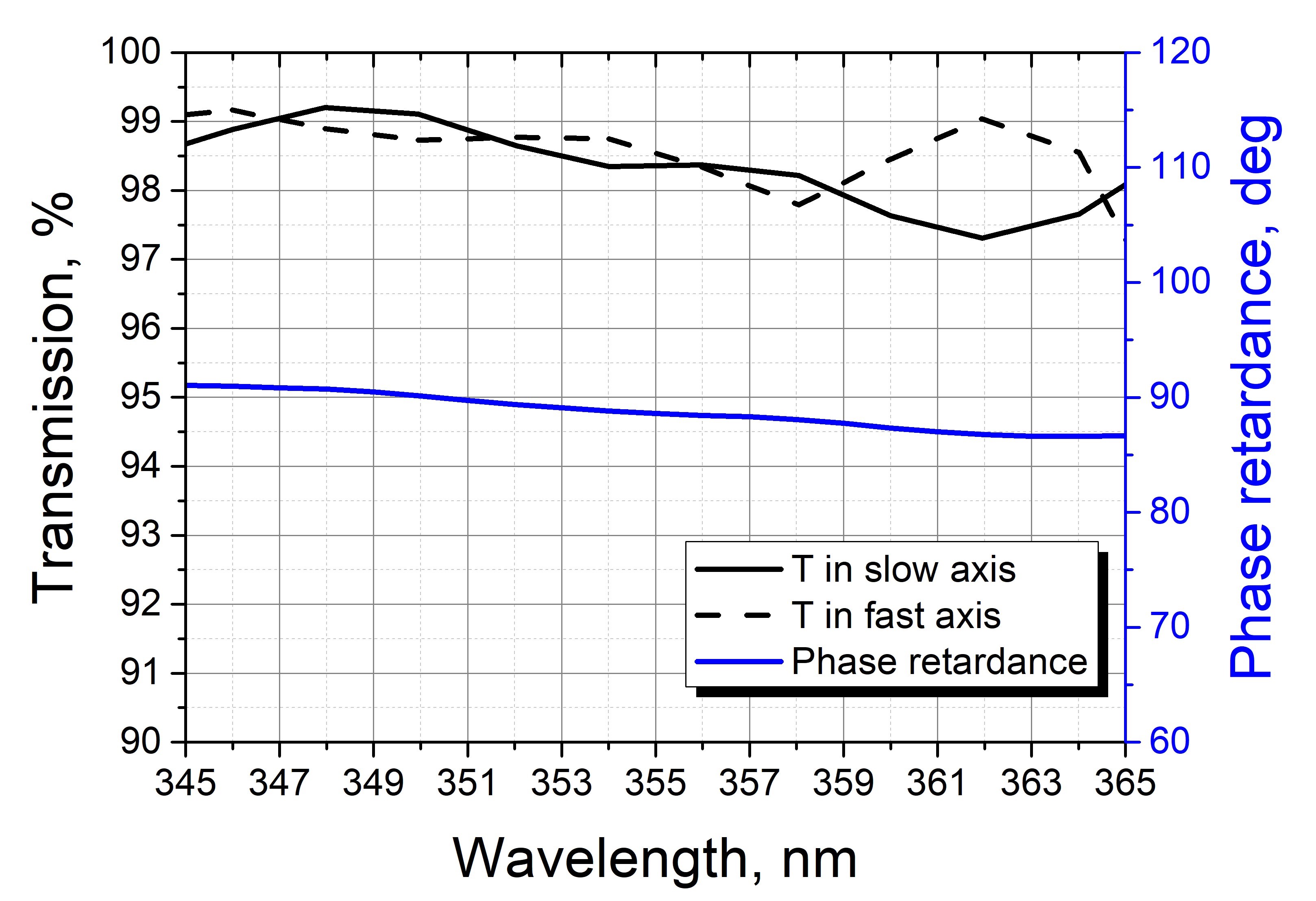
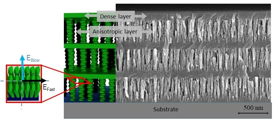
DESCRIPTION, INNOVATION AND ADVANTAGES
The glancing angle deposition technique is employed to form nanostructured anisotropic layers by evaporating amorphous materials. Placing the substrate at an oblique angle induces the self-shadowing effect, which causes the growth of columnar nanostructures with elliptical shape cross-sections. The combination of such porous birefringent layers with comparatively small refractive index and dense isotropic thin films with higher refractive index allows forming interference coatings with required properties – high transmission or high reflection. Furthermore, due to the birefringence in anisotropic layers, the needed phase delay difference of perpendicular polarizations can be achieved to form waveplates. Low optical losses and high transparency (T~99%) can be achieved while indicating the potential to withstand high laser fluence of 40 J/cm2 in a nanosecond regime at 355 nm wavelength. Moreover, true zero-order waveplates can be produced for any wavelength in the spectral range from UV to IR. Since it is a thin film-based component, it can be coated on any surface: nonlinear crystals, mirrors, glasses etc. The aforementioned flexibility allows applying such waveplates in both – large high-power facilities and microsystems.
CURRENT STAGE OF DEVELOPMENT*
Under development /laboratory tested.
INTELLECTUAL PROPERTY RIGHTS STATUS:
In-house know-how.
TYPE AND ROLE OF PARTNER SOUGHT:
Industrial and (or) research institutions.
CONTACT
Dr. Lina Grinevičiūtė
Phone +37062861306, e-mail: lina.grineviciute@ftmc.lt
CERAMIC FULL-COLOUR 3D PRINTING
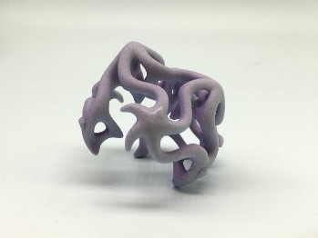
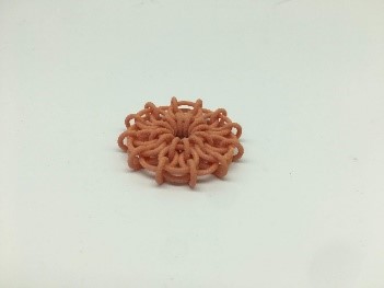
DESCRIPTION, INNOVATION AND ADVANTAGES
ColorJet Printing (CJP) is an additive manufacturing technology and it is an incomparable solution for full-colour concept model fabrication. The CJP ProJet 660Pro, using the ColorJet Printing technology, is a full-colour ceramic 3D printer for professional use. It can print to a resolution of 600x540 dpi and has a build size of 254x381x203 mm3. The printing speed is up to 28 mm3/h, and the minimum layer thickness is 0.1 mm. Using its 1520 jets and 5 print heads and the high-performance VisiJet PXL core and bonding materials, this 3D printer can create photo-realistic and precise colour models. It is used for ceramic and composite material research, production of highly complex geometry models and later aero and thermodynamic testing. Investigation of electroless catalytic copper plating on ceramic 3D surfaces has been performed and results have shown that the surface of objects manufactured using the ProJet 660Pro machine can be altered by successfully applying metal plating.
CURRENT STAGE OF DEVELOPMENT
Ready for work.
STATUS OF INTELLECTUAL PROPERTY RIGHTS
In–house know–how.
TYPE AND ROLE OF PARTNER SOUGHT
Architect, jewellery, art, companies.
CONTACT
Karolis Stravinskas
Phone +37067871496, e-mail: karolis.stravinskas@ftmc.lt
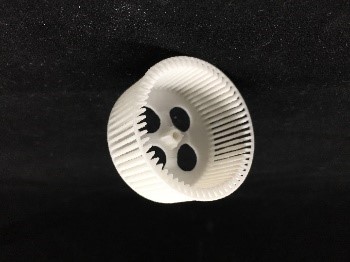
DIRECT METAL LASER SINTERING
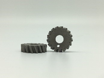
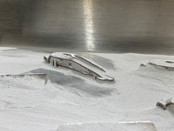
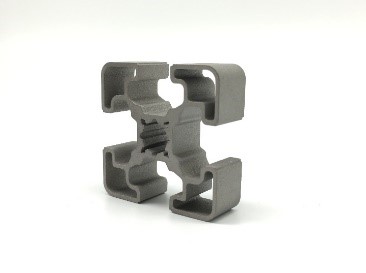
DESCRIPTION, INNOVATION AND ADVANTAGES
Direct Metal Laser Sintering (DMLS) is an additive manufacturing technology that is commercially used for metal part fabrication. This technology allows to manufacture of high accuracy strong and durable components of complex geometry and can be used for the fabrication of three-dimensional cooling channels, moulds or topologically optimised parts. Part fabrication, investigation of DMLS process and novel material testing are done applying the EOSINT M280 machine. The EOS EOSINT M280 is an industrial 3D printer based on DMLS 3D printing technology. This 3D printing technique uses a fibre laser to melt and fuse fine metal powder. The printer has a 200 W built-in Yb (Ytterbium) fibre laser with a wavelength of 1060-1100 nm. The maximum build size is 250x250x325 mm3. Different metal powders such as stainless steel, aluminium, cobalt-chromium or titanium can be used in the printing process using a layer thickness of 20 or 40 µm.
CURRENT STAGE OF DEVELOPMENT
Ready for work.
STATUS OF INTELLECTUAL PROPERTY RIGHTS
In–house know-how.
TYPE AND ROLE OF PARTNER SOUGHT
Space, aviation, automotive, medicine companies.
CONTACT
Ada Steponavičiūtė
Phone +37062607324, e-mail: ada.steponaviciute@ftmc.lt
LASER ABLATION TECHNOLOGY FOR THE FABRICATION OF THz OPTICAL COMPONENTS
DESCRIPTION, INNOVATION AND ADVANTAGES
This technology is used for the manufacture of diffractive silicon and metal lenses (zone plates) and metal resonance bandpass filters. Optical components for the 0.1 – 5 THz frequency range can be manufactured. The aperture of the optical element ranges from 10 to 25 mm.
CURRENT STAGE OF DEVELOPMENT
Technology validated in small series production.
STATUS OF INTELLECTUAL PROPERTY RIGHTS
In–house know-how.
TYPE AND ROLE OF PARTNER SOUGHT
Companies producing THz components.
CONTACT
Dr. Paulius Gečys
Phone +370 600 04346, e-mail: p.gecys@ftmc.lt
LASER DICING OF GLASS
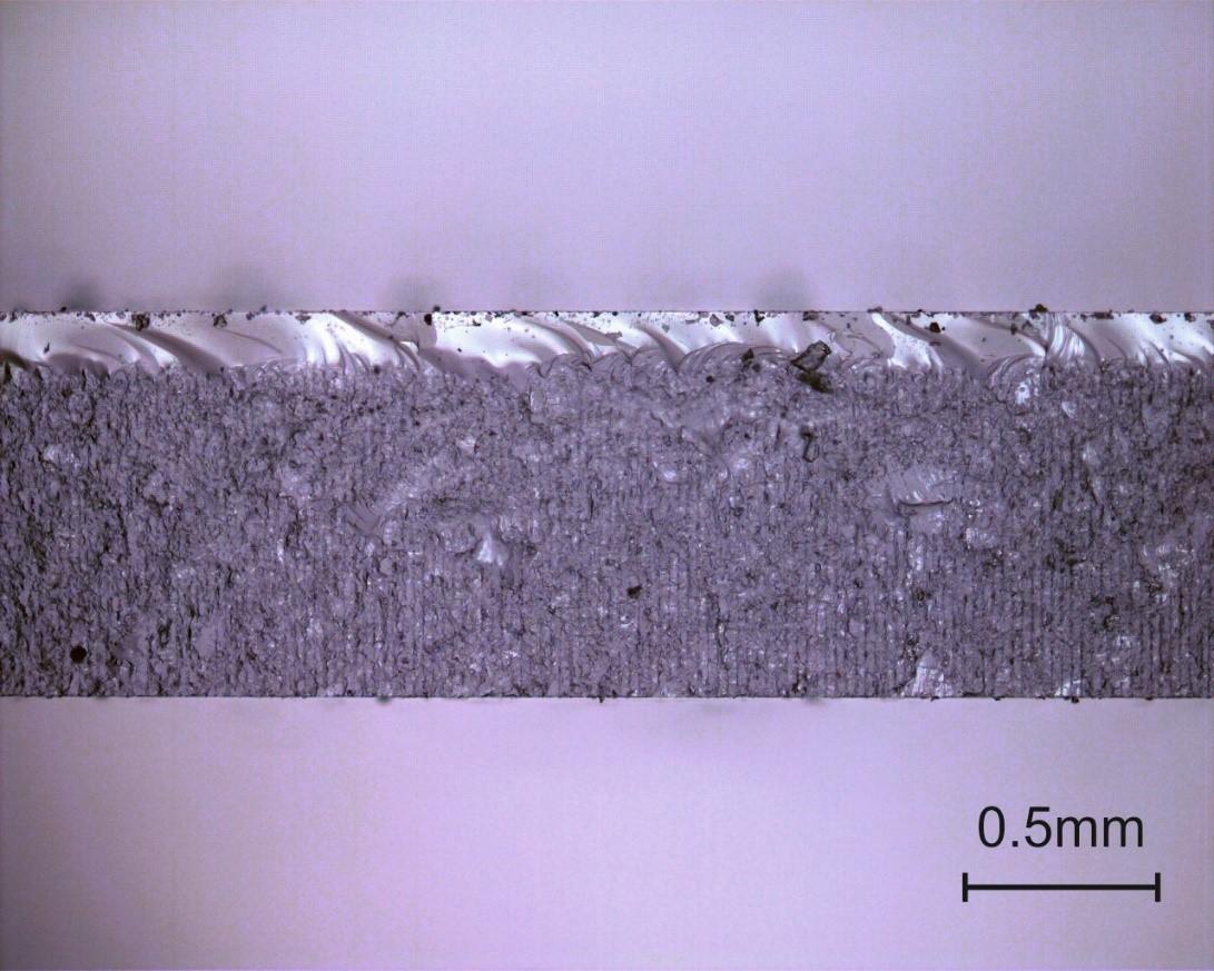
DESCRIPTION, INNOVATION AND ADVANTAGES
One of the most material-efficient and energy-efficient glass cutting techniques is to locally weaken the material along the cutting path by generating cracks or material modifications and then separating sheets by applying thermal or mechanical load. We demonstrate the possibility to cut glasses up to 5 mm thickness by applying laser-induced modifications. The cutting process can offer high cutting efficiency, where 1 mm thick glass sheet can be cut with a speed of 240 mm/s.
CURRENT STAGE OF DEVELOPMENT
Technology validated in small series production.
STATUS OF INTELLECTUAL PROPERTY RIGHTS
In–house know-how.
TYPE AND ROLE OF PARTNER SOUGHT
Hi-tech photonics companies.
CONTACT
Dr. Paulius Gečys
Phone +370 600 04346, e-mail: p.gecys@ftmc.lt
PRECISION PROCESSING OF GLASS BY LASER
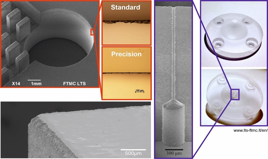
DESCRIPTION, INNOVATION AND ADVANTAGES
Laser-based techniques such as rear side glass processing can offer high quality and throughput, which can be used for glass drilling, cutting and milling applications. The laser milled feature sizes can be reduced to 150 µm. Laser cuts are taper-less, extremely high aspect ratio features can be fabricated. Laser-based processing can maintain high throughput with the highest processing quality keeping surface chipping below 100 µm.
Materials: soda-lime glass (SLG), fused silica, BK7 glass, borosilicate glass;
Quality: Surface chipping <100 µm, sidewall roughness <2 µm;
Cutting throughput: 0.6 m/min (1 mm SLG glass), 0.12 m/min (5 mm SLG glass);
Via drilling Ø 0.2-1 mm: 1 s/via (1 mm SLG), 5 s/via (5 mm SLG);
Material removal rate: >90 mm3/min.
CURRENT STAGE OF DEVELOPMENT
Technology validated in small series production.
INTELLECTUAL PROPERTY RIGHTS STATUS
Know-how and design rules.
TYPE AND ROLE OF PARTNER SOUGHT
Hi-tech photonics companies, producing specialized components from glass.
CONTACT
Dr. Paulius Gečys
Phone +370 600 04346, e-mail: p.gecys@ftmc.lt
METAL-DIELECTRIC COATINGS
DESCRIPTION, INNOVATION AND ADVANTAGES
Metal-dielectric coatings are widely used in various fields from optical, electro-optical elements to laser and sensor applications. It might be prepared protected and enhanced high-reflective mirrors. Such coatings are usually consisting of several metal and dielectric layers. It was developed a unique technology in order to produce such structures with very high precision, especially in the metal layer.
Our special process control technologies let to prepare desired coatings. It is possible to reach very high precision in every layer. This technology is based on the combination of stable film deposition and special film growth monitoring.
There is a possibility to prepare the various coating, using materials like Ag, Au, Cu, Al and many others. The final results might be modelled in advance.
CURRENT STAGE OF DEVELOPMENT
Available for demonstration.
Prototype available for demonstration.
STATUS OF INTELLECTUAL PROPERTY RIGHTS
In-house know-how, granted patent.
TYPE AND ROLE OF PARTNER SOUGHT
Industrial and (or) research institutions.
CONTACT
Dr. Alexandr Belosludtsev
E-mail: belosludtsev@ftmc.lt
PLASMA ETCHING OF POLISHED GLASS AND CRYSTAL SUBSTRATES FOR PREPARING HIGH POWER LASER COMPONENTS
DESCRIPTION, INNOVATION AND ADVANTAGES
Our plasma etching technology targets the essential improvement of polished optical substrates (glasses, crystals) in order to increase their laser damage resistance and produce coated transparent optical components for high power laser applications.
The subsurface of polished substrates very often contains the so-called Beilby layer, contaminated with polishing residuals. This sub-layer effectively absorbs laser radiation (especially in UV spectral range) and becomes the weakest link of laser component coated with antireflection (AR) or any other type of transmitting dielectric coating (beam splitter, polarizer, etc.).
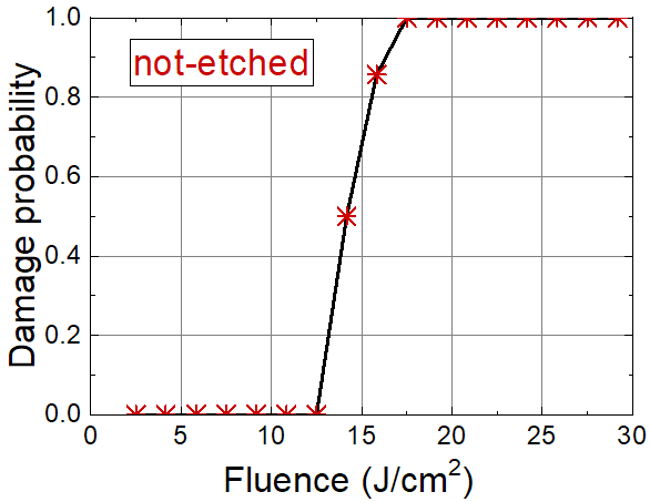
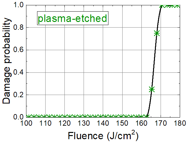
Developed low-energy plasma etching allows effective removal of this contaminated substrate subsurface layer. Extensive studies demonstrated an increase of fused silica (FS) substrate laser-induced damage threshold (LIDT) from initial 20 J/cm2 up to 100-150 J/cm2 (355 nm, 2 ns duration laser pulse, test 1-on-1) after plasma etching. Another advantage is that initial substrate surface roughness is maintained after the etching procedure. Plasma etched and coated with AR coating FS substrate demonstrated the increase of 3.4x of LIDT for 355nm laser pulse compared with unprocessed and simultaneously coated FS substrate. Developed technology was also further applied for the etching of various non-linear and laser crystals, such as spinel (MgAl2O4), BSO, YAG. A significant (at least 2-3 times) increase of their LIDT in the near-infrared spectral range was obtained. Several successful collaborations with industrial partners were executed.
CURRENT STAGE OF DEVELOPMENT
Field tested / evaluated
Available for demonstration
Prototype available for demonstration
STATUS OF INTELLECTUAL PROPERTY RIGHTS
In-house know-how.
TYPE AND ROLE OF PARTNER SOUGHT
Industrial and (or) research institutions.
CONTACT
Dr. Giedrius Abromavičius
Phone +37060411153, e-mail: giedrius.abromavicius@ftmc.lt
LASER-INDUCED SELECTIVE PLATING OF DIELECTRICS FOR ELECTRONIC CIRCUIT FABRICATION
DESCRIPTION, INNOVATION AND ADVANTAGES
Electric circuit traces formation on 3D shaped dielectrics is one of the biggest challenges in 3D Mechatronic Integrated Devices (3D-MID). The advanced technology of Selective Surface Activation Induced by a Laser (SSAIL) can solve emerged production issues for electric traces. The process can be applied almost on any commercial dielectric material by adapting laser and chemical parameters. Narrow copper lines below one micrometre in a width) are feasible to produce. The technology is capable to fabricate a metallic mesh with metal wires less than 5 µm in diameter to be invisible but still electro-conductive. Therefore, such metallic mesh can substitute Indium Tin Oxide (ITO) in the transparent conductive film market.
CURRENT STAGE OF DEVELOPMENT
Ready for the integration in production lines.
STATUS OF INTELLECTUAL PROPERTY RIGHTS
Patented (WO 2018051210; JP 6749482; LT 6518; US 10982328; EP 3512980; CN 109844178; KR 102319221
TYPE AND ROLE OF PARTNER SOUGHT
- Industrial Electronics manufacturers.
- Partners for global marketing.
CONTACT
Dr. Karolis Ratautas
Phone +370 618 42061; e-mail: karolis.ratautas@ftmc.lt
CONVERSION OF CO2 INTO USEFUL MATERIALS
DESCRIPTION, INNOVATION AND ADVANTAGES
Carbon dioxide (CO2) is the most common greenhouse gas in our planet. Reduction of CO2 production and conversion of CO2 into useful materials at the same time is necessary. Our proposed technology enables CO2 conversion using electrocatalysis and can be controlled by electrode potentials and the reaction temperature. This process produces higher hydrocarbons such as ethanol, methanol and others. Also, the electrochemical reaction systems are compact, modular and easy for scale-up applications. This system uses in-house developed Cu-based composites as catalysts with different compositions can seriously influence its electrocatalytic performance toward CO2 reduction reaction.
CURRENT STAGE OF DEVELOPMENT
Ready for the integration in production lines after scale-up development.
STATUS OF INTELLECTUAL PROPERTY RIGHTS
In-house know-how
TYPE AND ROLE OF PARTNER SOUGHT
- Industrial reactors or clean fuel manufacturers.
- Partners for global marketing.
CONTACT
Karolis Stašys
Phone +370 629 85166; e-mail: karolis.stasys@ftmc.lt