Innovations
- Home
- Innovations
- Services
- Optical Coatings
Tired of your laser components burning out? No more!
.JPG)
FTMC has decades of experience developing and manufacturing optical coatings for various applications and wavelengths. Just tell us the purpose and desired wavelength and we will manufacture the coating which perfectly suits your needs. Here is an example our technologies developed and services:
All-silica based mirrors for high power laser applications
A principal possibility to overcome fundamental (intrinsic) limit of pure optical materials laser light resistance is achieved by designing artificial materials with desired optical properties. Technology to form all-silica high reflection mirrors, are developed at Optical Coatings Laboratory using glancing angle deposition method. A structural and optical investigation indicates the advanced properties of SiO2 coatings. The comparing with conventional coatings shows a significant increase in laser induced damage threshold. Extended investigation of fabrication method also enables to fabricate more complex optical components. Novel approach indicates the potential for coating to withstand laser fluence of at least 65 J/cm2 without reaching intrinsic threshold value. Technology allows to form the wide range of optical components, ranging from UV mirrors, AR coatings to spectral filters at NIR spectral region.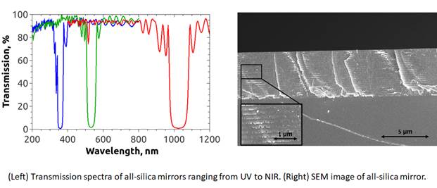
Plasma etching of optical glasses and crystals for high power transmitting optical component application
Our plasma etching technology aims for essential improvement of optical substrates (glasses, crystals) preparation in order to produce transmitting optical components for high power laser applications.
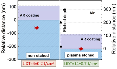
Subsurface of polished substrates very often contains so-called Beilby layer, contaminated with polishing residuals. This layer, coated with antireflection (AR) or other type of transmitting dielectric coating (beam splitter, polarizer, etc.), absorbs laser radiation and causes damage under relevant laser fluency.
Our developed low-energy plasma etching allows to remove this contaminated substrate subsurface layer. Studies show, that laser induced damage threshold (LIDT) increases up to 3-4 times in UV range while up to 2 times in NIR range (for uncoated substrate). Chosen low plasma energy also enables gentle surface removal and maintains initial substrate surface roughness after the etching procedure. Etched and coated with AR coating elements demonstrated increase of 3.4 times of LIDT for 355nm ns laser pulses. Developed etching technology was also successfully applied for preparation of several different crystals, significantly increasing their LIDT with the coatings for near-infrared spectral range.
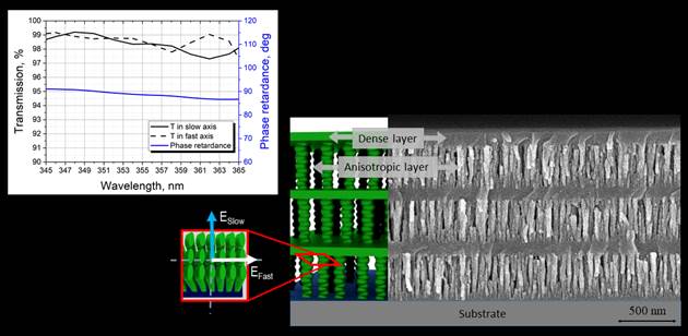
True zero-order waveplates based on all-silica thin films
Glancing angle deposition technique can be employed to form nano-structured anisotropic layers by evaporating amorphous materials. Placing the substrate at oblique angle induces the self-shadowing effect, which causes the growth of tilted columnar nano-structures with elliptical shape cross-sections. Combination of such porous birefringent layers with comparatively small refractive index and dense isotropic thin films with higher refractive index allows to form interference coatings with required properties – high transmission or high reflection. Furthermore, due to the birefringence in anisotropic layers, the needed phase delay difference of perpendicular polarizations can be achieved to form waveplates. Low optical losses and high transparency (T~99%) can be achieved while indicating potential to withstand high laser fluence of 40 J/cm2 in nanosecond regime at 355 nm wavelength. Moreover, true zero-order waveplates can be produced for any wavelength in the spectral range from UV to IR. Since it is a thin film based component, it can be coated on any surface: nonlinear crystals, mirrors, glasses etc. Aforementioned flexibility allows to apply such waveplates in both – large high-power facilities and microsystems.
Metal-dielectric coatings
Metal-dielectric coatings might be widely used in various fields from optical elements to sensor applications. Such coatings are usually consist of several metal and dielectric layers. And there is a big challenge to produce such structures with very high precision, especially for metal layer. Even very small errors during the layer deposition might easily induce errors in the whole coating.
Our special process control technologies let to prepare desired coatings with the precision up to nanometre level. This technology is based on the combination of the sputtering process and special film growth monitoring. The sputtering technology is rather developed and well established. It is well known by the high coating density and process repeatability.
Our special solution refers to the special monitoring technology that is based on the in-situ control of the metal film growth. We have precisely characterized various metal films. Metal films on dielectric surface might be formed in the form of: 1) separate islands; ii) coalescence islands and iii) continuous film. Depending on request such structures might be controllably produced.
Coatings for the infrared range
Silicon is the material of interest in 3-5 micron band and germanium is the widely used material in 8-12 microns band.
We have developed the technology for such coatings preparation by sputtering process. The sputtering technology is rather developed and well established. It is well known by the high coating density and process repeatability.
We have developed the technology for such coatings preparation by sputtering process. The sputtering technology is rather developed and well established. It is well known by the high coating density and process repeatability.
During the deposition we apply process monitoring technology in order to get high process precision. Additionally we have precisely characterized various semiconductor films and we have possibility to model and demonstrate spectra of desired structures.
Don’t wait until your lasers burns out – order now!
.JPG)
.JPG)
Contact us
Contact us by filling out the inquiry form. We will respond within 2 business days.
Karolis Stašys
Innovation Manager / Inovacijų vadybininkas
Tel.: +370 629 85166
El.p.: karolis.stasys@ftmc.lt