Structure
- Home
- Structure
- Scientific Divisions
- Department of Optoelectronics
- Photonic Technologies and Devices Laboratory
Photonic Technologies and Devices Laboratory
Head of the laboratory dr. Vaidas Pačebutas
phone +370 5 2627469
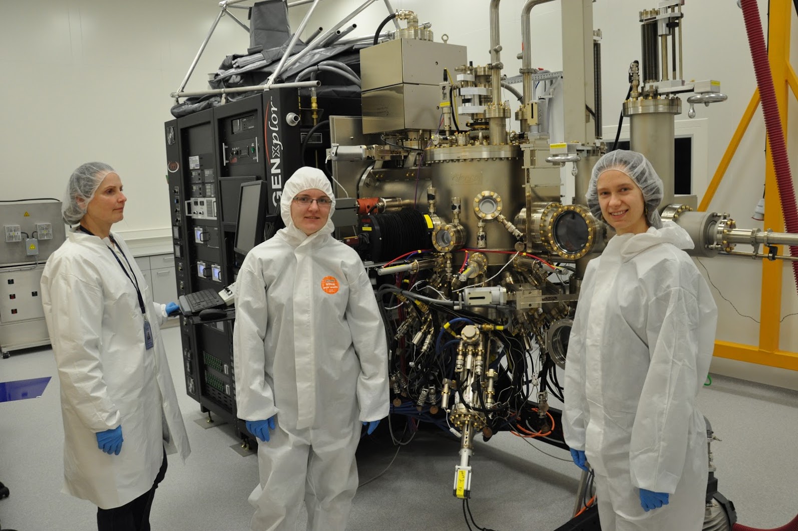
The activity of laboratory covers the development of molecular beam epitaxy (MBE) technologies, development of optoelectronic devices, gathering new knowledge, and improvement of level of expertise of the Laboratory stuff.
The main tasks:
- Investigation of growth conditions of layers and quantum structures of bismides including GaAsBi, InGaAsBi, InAsBi and other A3B5 compounds, optimization of physical parameters convenient for optoelectronic devices fabrication.
- Complex investigations of physical properties to empower the relation with technological conditions, development of investigation methods.
- The development, optimization and manufacturing of new optoelectronic devices such as terahertz emitters and detectors, UTC diodes, semiconductor LED’s and lasers for infrared region.
 |
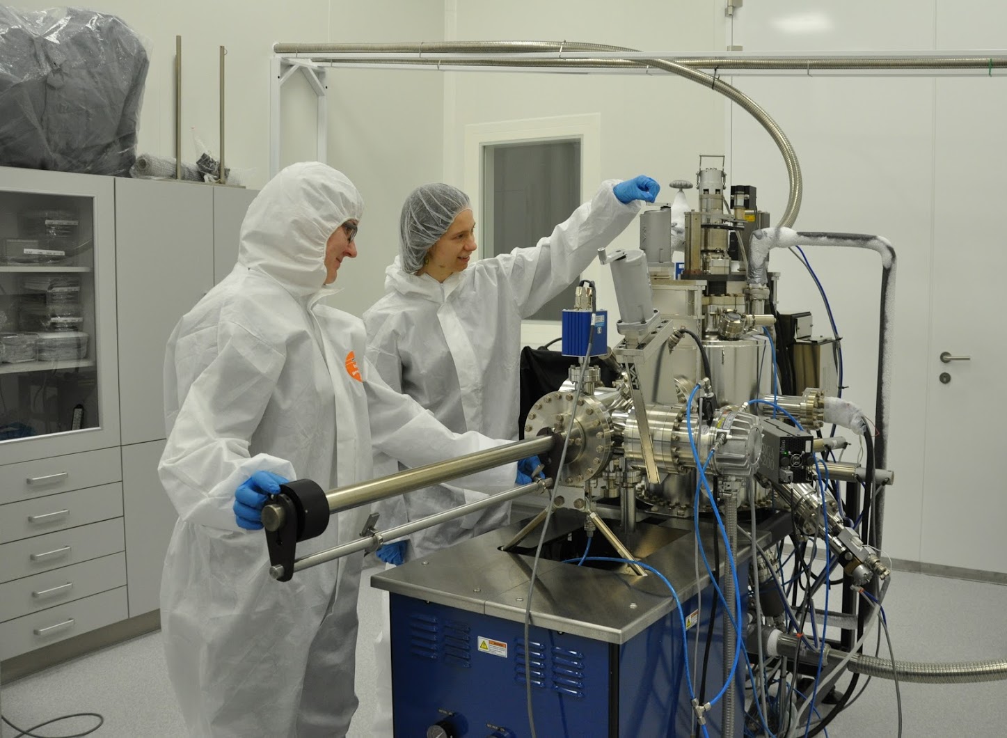 |
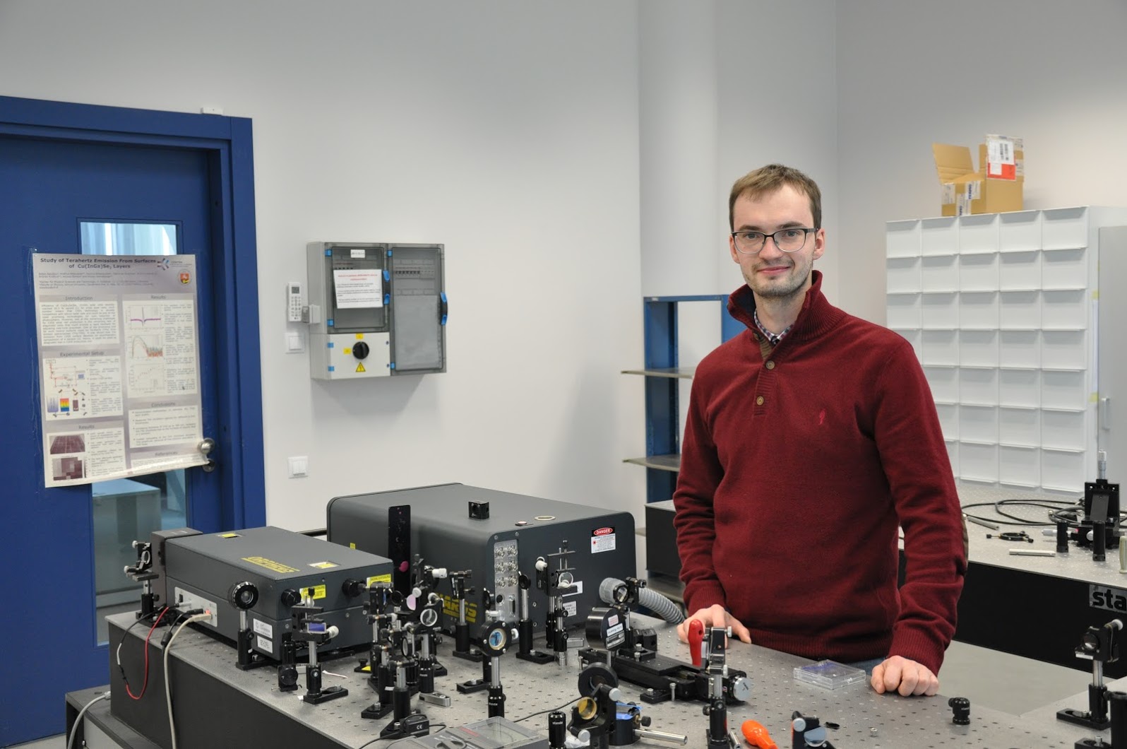
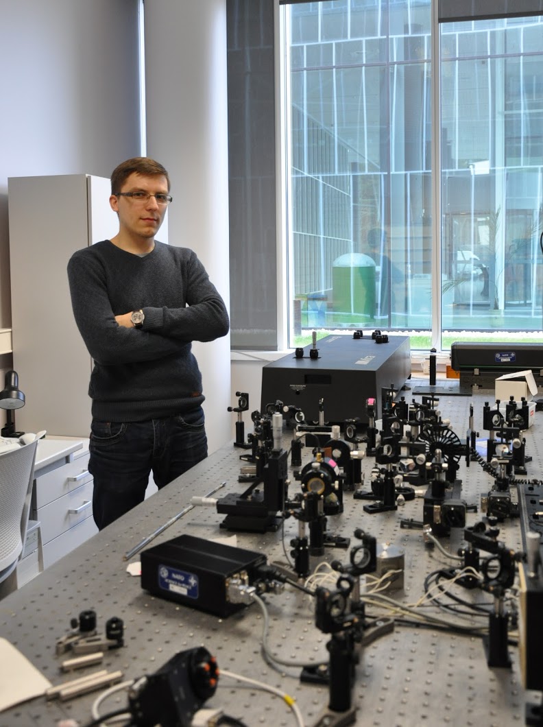
Laboratory has expertise in the field of ultrafast carrier dynamics in semiconductors and semiconductor devices; its staff has developed several experimental techniques based on the use of femtosecond pulsed lasers. Researchers of the Laboratory have investigated THz pulse emission from the surfaces of various semiconductors excited by femtosecond laser pulses, developed efficient optoelectronic emitters and detectors of such pulses. They are also active in search for new fields of application of the THz spectroscopy application.
 |
 |